
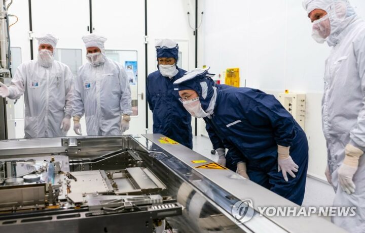
Historic deal with ASML to help Samsung gain advantage in 2nm chips
A few weeks ago, Samsung Electronics boss Lee Jae-yong embarked on a business trip to the Netherlands to make important business deals with semiconductor chip equipment maker ASML. He joined the South Korean president on a 4-day official trip after the Dutch King Willem-Alexander invited them to the Netherlands to discuss several chip deals.
Samsung is satisfied with the semiconductor chip deals it signed with ASML
Yesterday, Lee Jae-yong returned from the Netherlands to Seoul, South Korea, and he expressed his satisfaction to the press about the business deals signed with the Dutch firm ASML. Lee said that most of the achievements made there were focused on semiconductor chips. If you don’t know already, ASML is the only firm that makes advanced EUV (Extreme Ultraviolet) chip-making equipment of 7nm or better. Each such EUV machine costs millions of dollars, and ASML can only make 40-50 such machines. Acquiring those machines has become a lot harder for chip-making firms like Samsung and TSMC.
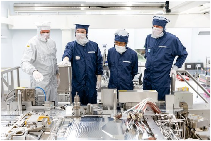
Samsung Electronics signed a KRW 1 trillion ($755 million) deal with ASML last week. The two companies will invest in building a semiconductor chip research plant in South Korea, where EUV technologies will be developed. Samsung Electronics Vice Chairman Kyung Kye-hyun, who heads the Device Solutions Division, emphasized that the company’s latest agreements will help it secure next-generation High-NA (Numerical Aperture) EUV lithography scanner equipment.
Kyung said, “Samsung has secured a priority over the High-NA equipment technology. (From the trip), I believe we created an opportunity for us to optimize the usage of High-NA technology for our production of DRAM memory chips and logic chips in the long term.”
In the upcoming chip research facility in Dongtan, Gyeonggi Province, South Korea, engineers from ASML and Samsung Electronics will work together to improve the EUV chip fabrication technology. Rather than focusing on bringing 2nm chip-making equipment to South Korea, Samsung’s deal with ASML focuses on building a partnership with the Dutch firm so that it can make better use of next-generation equipment.
ASML plans to launch ten 2nm chip-making equipment next year
ASML will launch the equipment to make 2nm node chips in the coming months. The latest equipment will increase the light collecting capability from 0.33 to 0.55, which will allow chip makers to use ultrafine patterning technology to make 2nm-node chips. ASML plans to make ten such equipment next year, and Intel is said to have acquired six of those machines. In the coming years, ASML is planning to improve the production capacity of such chips to 20 per year.
After acquiring 2nm chip equipment from ASML, Samsung plans to start the production of 2nm chips in late 2025. However, as with any technology and strategic plan, there could be delays in the launch of such chips, depending on the market condition and the quality of production. Rather than focusing on
A few weeks ago, Samsung Electronics boss Lee Jae-yong embarked on a business trip to the Netherlands to make important business deals with semiconductor chip equipment maker ASML. He joined the South Korean president on a 4-day official trip after the Dutch King Willem-Alexander invited them to the Netherlands to discuss several chip deals.
Samsung is satisfied with the semiconductor chip deals it signed with ASML
Yesterday, Lee Jae-yong returned from the Netherlands to Seoul, South Korea, and he expressed his satisfaction to the press about the business deals signed with the Dutch firm ASML. Lee said that most of the achievements made there were focused on semiconductor chips. If you don’t know already, ASML is the only firm that makes advanced EUV (Extreme Ultraviolet) chip-making equipment of 7nm or better. Each such EUV machine costs millions of dollars, and ASML can only make 40-50 such machines. Acquiring those machines has become a lot harder for chip-making firms like Samsung and TSMC.
Samsung Electronics signed a KRW 1 trillion ($755 million) deal with ASML last week. The two companies will invest in building a semiconductor chip research plant in South Korea, where EUV technologies will be developed. Samsung Electronics Vice Chairman Kyung Kye-hyun, who heads the Device Solutions Division, emphasized that the company’s latest agreements will help it secure next-generation High-NA (Numerical Aperture) EUV lithography scanner equipment.
Kyung said, “Samsung has secured a priority over the High-NA equipment technology. (From the trip), I believe we created an opportunity for us to optimize the usage of High-NA technology for our production of DRAM memory chips and logic chips in the long term.”
In the upcoming chip research facility in Dongtan, Gyeonggi Province, South Korea, engineers from ASML and Samsung Electronics will work together to improve the EUV chip fabrication technology. Rather than focusing on bringing 2nm chip-making equipment to South Korea, Samsung’s deal with ASML focuses on building a partnership with the Dutch firm so that it can make better use of next-generation equipment.
ASML plans to launch ten 2nm chip-making equipment next year
ASML will launch the equipment to make 2nm node chips in the coming months. The latest equipment will increase the light collecting capability from 0.33 to 0.55, which will allow chip makers to use ultrafine patterning technology to make 2nm-node chips. ASML plans to make ten such equipment next year, and Intel is said to have acquired six of those machines. In the coming years, ASML is planning to improve the production capacity of such chips to 20 per year.
After acquiring 2nm chip equipment from ASML, Samsung plans to start the production of 2nm chips in late 2025. However, as with any technology and strategic plan, there could be delays in the launch of such chips, depending on the market condition and the quality of production. Rather than focusing on
Denial of responsibility! Techno Blender is an automatic aggregator of the all world’s media. In each content, the hyperlink to the primary source is specified. All trademarks belong to their rightful owners, all materials to their authors. If you are the owner of the content and do not want us to publish your materials, please contact us by email – [email protected]. The content will be deleted within 24 hours.