Nvidia’s Hopper H100 SXM5 Pictured: Monstrous GPU Has Brutal VRM Config
Modern compute GPUs are tailored to deliver incredible performance at any cost, so their power consumption and cooling requirements are pretty enormous. Nvidia’s latest H100 compute GPU based on the Hopper architecture can consume up to 700W in a bid to deliver up to 60 FP64 Tensor TFLOPS, so it was clear from the start that we were dealing with a rather monstrous SXM5 module design. Yet, Nvidia has never demonstrated it up and close.
Our colleagues from ServeTheHome, who were lucky enough to visit one of Nvidia’s offices and see an H100 SXM5 module themselves, on Thursday published a photo of the compute GPU. These SXM5 cards are designed for Nvidia’s own DGX H100 and DGX SuperPod high-performance computing (HPC) systems as well as machines designed by third parties. These modules will not be available separately in retail, so seeing them is a rare opportunity.
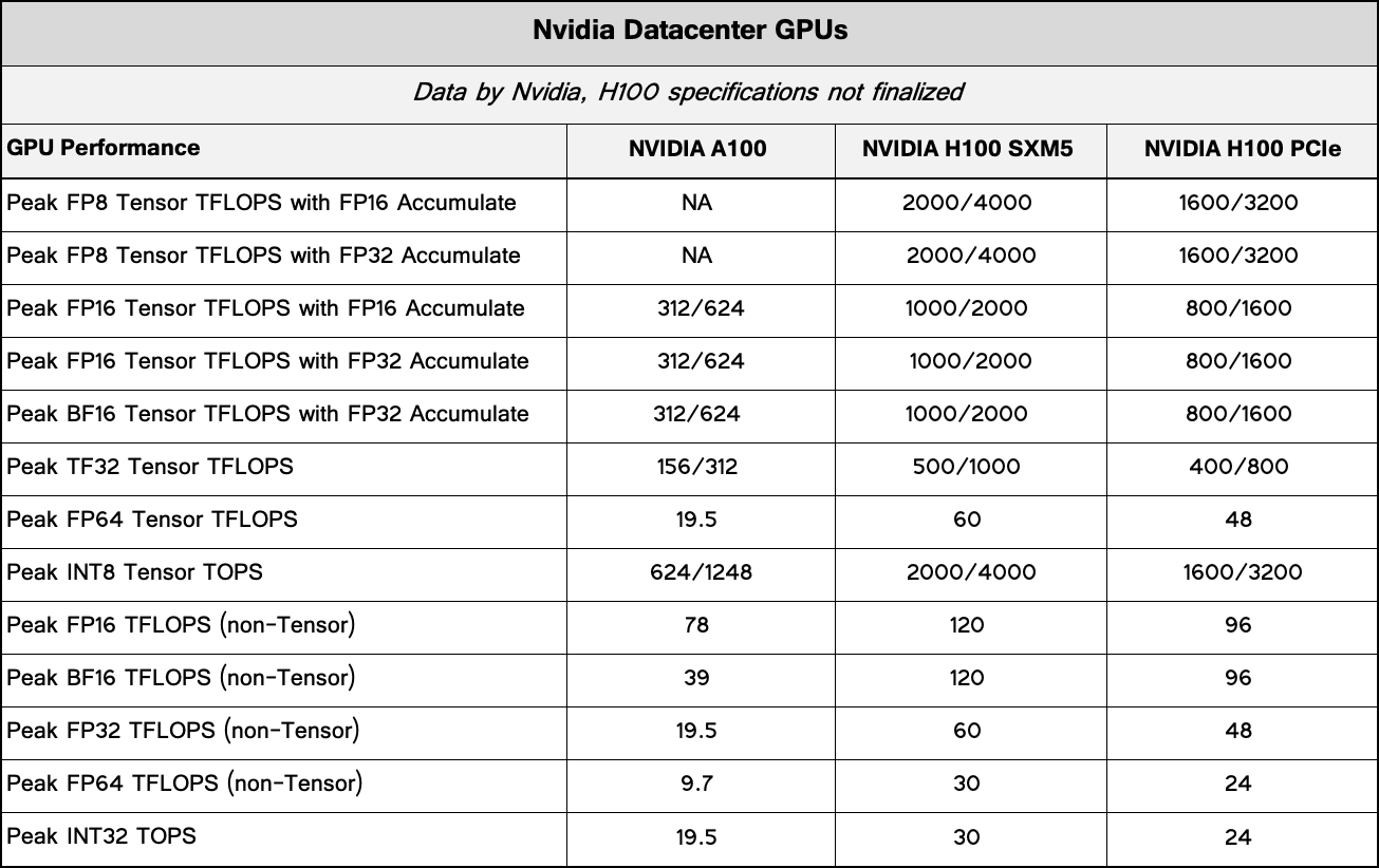
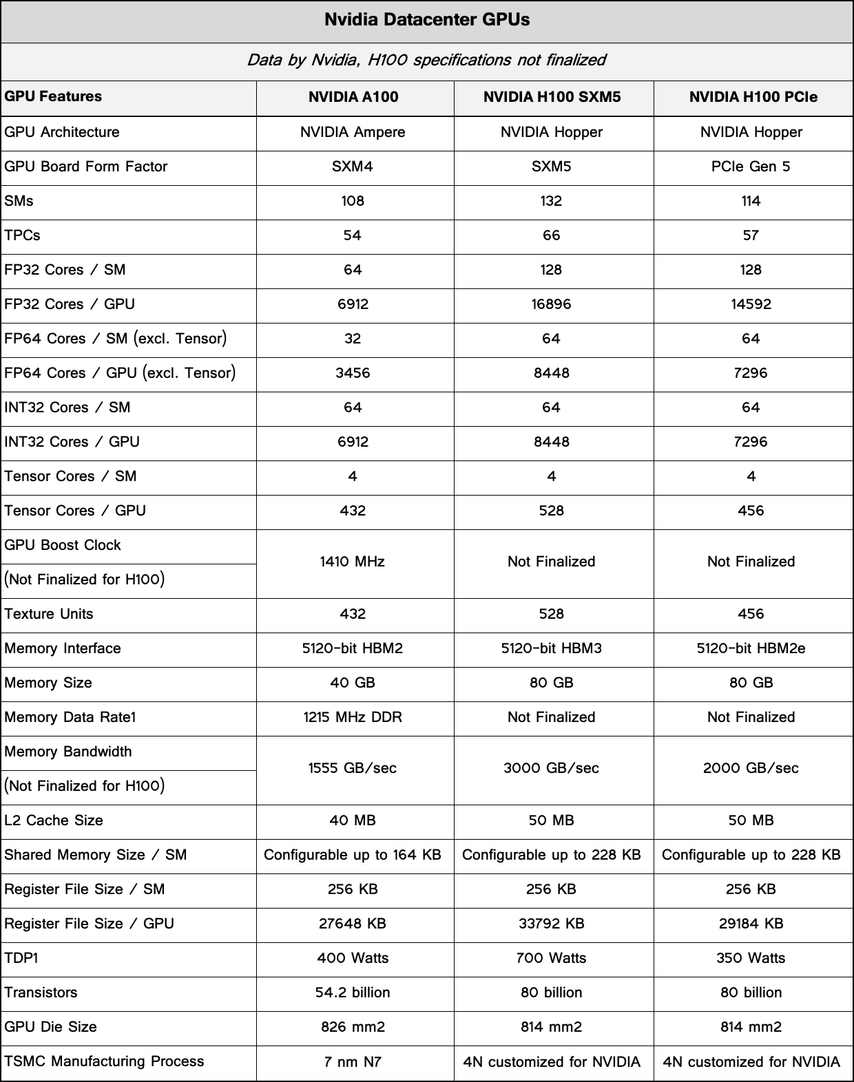
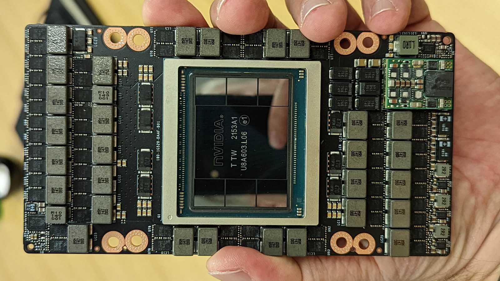
Nvidia’s H100 SXM5 module carries a fully-enabled GH100 compute GPU featuring 80 billion transistors and packing 8448/16896 FP64/FP32 cores as well as 538 Tensor cores (see details about specifications and performance of H100 in the tables below). The GH100 GPU comes with 96GB of HBM3 memory, though because of ECC support and some other factors, users can access 80GB of ECC-enabled HBM3 memory connected using a 5120-bit bus. The particular GH100 compute GPU pictured is A1 revision marked as U8A603.L06 and packaged on the 53rd week of 2021 (i.e., from December 28 to December 31).
Nvidia’s GH100 measures 814mm^2, which makes it one of the largest chips ever made. In fact, die sizes of Nvidia’s recent compute GPUs were primarily limited by reticle size of modern semiconductor production tools, which is around 850mm^2. Since the chip made using a customized TSMC N4 process technology (which belongs to the N5 family of nodes) consists of 80 billion transistors operating at around 1.40 ~ 1.50 GHz, the GPU is extremely power hungry. Nvidia rates its thermal design power at 700W (yet this number can change), so it requires an extremely sophisticated voltage regulating module (VRM) that can deliver enough power to feed the beast.
Indeed, the H100 SXM5 module comes with a VRM that has 29 high current inductors each equipped with two power stages as well as three inductors with one power stage. The inductors can survive high temperatures for prolonged periods of time and they come in metal shells to make VRM cooling easier.
Dimensions of the SXM5 module are unknown, but they hardly differ significantly from previous-generation Nvidia modules for compute GPUs. Meanwhile, Nvidia changed the connector layout for SXM5 (check it out at ServeTheHome), probably because of higher power consumption and faster PCIe Gen5 and NVLink data rates supported by its GH100.
Nvidia will start commercial shipments of its Hopper H100 compute GPUs sometimes in the second half of this year and this is when it announces final specifications of these products and their final TDP.

Modern compute GPUs are tailored to deliver incredible performance at any cost, so their power consumption and cooling requirements are pretty enormous. Nvidia’s latest H100 compute GPU based on the Hopper architecture can consume up to 700W in a bid to deliver up to 60 FP64 Tensor TFLOPS, so it was clear from the start that we were dealing with a rather monstrous SXM5 module design. Yet, Nvidia has never demonstrated it up and close.
Our colleagues from ServeTheHome, who were lucky enough to visit one of Nvidia’s offices and see an H100 SXM5 module themselves, on Thursday published a photo of the compute GPU. These SXM5 cards are designed for Nvidia’s own DGX H100 and DGX SuperPod high-performance computing (HPC) systems as well as machines designed by third parties. These modules will not be available separately in retail, so seeing them is a rare opportunity.
Nvidia’s H100 SXM5 module carries a fully-enabled GH100 compute GPU featuring 80 billion transistors and packing 8448/16896 FP64/FP32 cores as well as 538 Tensor cores (see details about specifications and performance of H100 in the tables below). The GH100 GPU comes with 96GB of HBM3 memory, though because of ECC support and some other factors, users can access 80GB of ECC-enabled HBM3 memory connected using a 5120-bit bus. The particular GH100 compute GPU pictured is A1 revision marked as U8A603.L06 and packaged on the 53rd week of 2021 (i.e., from December 28 to December 31).
Nvidia’s GH100 measures 814mm^2, which makes it one of the largest chips ever made. In fact, die sizes of Nvidia’s recent compute GPUs were primarily limited by reticle size of modern semiconductor production tools, which is around 850mm^2. Since the chip made using a customized TSMC N4 process technology (which belongs to the N5 family of nodes) consists of 80 billion transistors operating at around 1.40 ~ 1.50 GHz, the GPU is extremely power hungry. Nvidia rates its thermal design power at 700W (yet this number can change), so it requires an extremely sophisticated voltage regulating module (VRM) that can deliver enough power to feed the beast.
Indeed, the H100 SXM5 module comes with a VRM that has 29 high current inductors each equipped with two power stages as well as three inductors with one power stage. The inductors can survive high temperatures for prolonged periods of time and they come in metal shells to make VRM cooling easier.
Dimensions of the SXM5 module are unknown, but they hardly differ significantly from previous-generation Nvidia modules for compute GPUs. Meanwhile, Nvidia changed the connector layout for SXM5 (check it out at ServeTheHome), probably because of higher power consumption and faster PCIe Gen5 and NVLink data rates supported by its GH100.

Nvidia will start commercial shipments of its Hopper H100 compute GPUs sometimes in the second half of this year and this is when it announces final specifications of these products and their final TDP.
