
Russian University Vows to Build 7nm-Capable Litho Tools by 2028
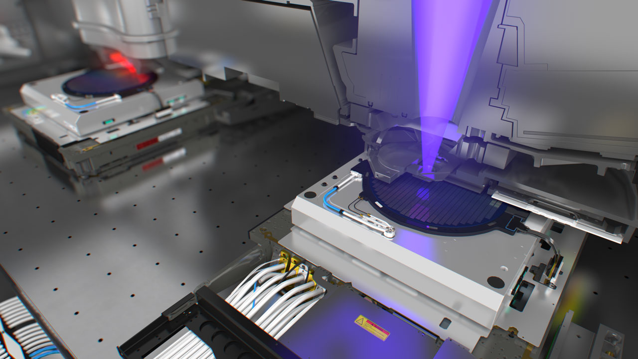
A Russian institute is developing its own lithography scanner that could produce chips using 7nm-class fabrication technologies. The machine is under development, with the plan to build it by 2028. When it is ready, it should be more efficient than ASML’s Twinscan NXT:2000i tool, whose development took over a decade.
After Russia unleashed its bloody war against Ukraine on February 24, Taiwan was quick to ban shipments of advanced chips to the nation. The U.S., the U.K., and the E.U. then followed up with sanctions that effectively prohibit virtually all contract chipmakers with advanced fabs from working with Russian entities. In addition, companies like Arm cannot license their technologies to Russia-based chip designers. As a result, the Russian government rolled out a national program to develop the country’s own 28nm-class fabrication technology by 2030, reverse engineer as many foreign chips as possible, and educate local talent to work on domestic chips.
However, there is a problem with a 28nm-class production node by 2030. Russia’s most advanced fab can produce chips using a 65nm fabrication technology. Meanwhile, American and European makers of fab tools cannot supply their equipment to Russia due to sanctions, so the country has to design and build domestic wafer production equipment if it wants to adopt a 28nm node. Essentially, what has taken companies like ASML and Applied Materials decades to develop and iterate has to be done in about eight years.
Apparently, the Russian Institute of Applied Physics of the Russian Academy of Sciences intends to beat all expectations and produce a 7nm-capable lithography scanner by 2028, according to its plans published on Nizhy Novgorod Strategy Development website (via CNews).
A modern lithography scanner capable of processing wafers using a 7nm-class process technology is a highly complex apparatus that involves a high-performance light source, sophisticated optics, and precise metrology, just to name a few critical parts. However, as a leading applied physics university in Russia, IAP believes that it can develop such a tool in a relatively short amount of time.
The tool will be somewhat different from scanners produced by companies like ASML or Nikon. For example, IAP plans to use a >600W light source (total power, not intermediate focus power) with an 11.3nm exposure wavelength (EUV wavelength is 13.5nm), which will require considerably more sophisticated optics than exists today. Because the light source of the device will be relatively low power, it will make the tool more compact and easier to build. Yet, it also means that its production of the scanner will be considerably lower than that of modern deep ultraviolet (DUV) tools. That might now be a problem, according to IAP.
“ASML, the global lithography leader, has been developing its EUV lithography system for almost 20 years and the technology has turned out to be incredibly complex,” said Nikolai Chkhalo, Deputy Director of the Institute of Physics of Microstructures of the Russian Academy of Sciences for scientific and technological development. “The main objective of ASML in this case was to maintain the extremely high productivity that is needed only at the world’s largest factories. In Russia, no one needs such high productivity. In our work, we start from the needs and tasks faced by domestic microelectronics — and this is not so much about quantity, but about quality. First of all, we need to transit to our own fabrication processes, develop our own design standards, our own tools, engineering, materials, so our own path is inevitable here. In fact, we need to balance between simplicity and performance.”
IAP plans to build a fully functional alpha scanner by 2024. This one will not have to offer high productivity or maximum resolution but will have to work and be attractive to potential investors. IAP intends to build a beta version of the scanner with higher productivity and resolution by 2026. This machine should be mass production ready, but its productivity is not expected to be at its maximized. The final iteration of the litho scanner is said to emerge in 2028. It should get a high-performance light source (hence better productivity), better metrology and overly capabilities. There is no word how many of such machines IAP and/or its production partners will be able to produce by 2028.
It should be noted that fab equipment is not limited to lithography scanners. There are other types of machines performing etching, deposition, resist removal, metrology, and inspection operations that are not made in Russia. Furthermore, there is somewhat less advanced machinery like ultrapure air and water generators which also are not produced in Russia. Even if IAP RAS manages to build a lithography tool, Russia will still be a few hundred tools short of building a modern fab. Also, fabs need ultrapure raw materials produced in countries that will not supply to Russia.
Denial of responsibility! Techno Blender is an automatic aggregator of the all world’s media. In each content, the hyperlink to the primary source is specified. All trademarks belong to their rightful owners, all materials to their authors. If you are the owner of the content and do not want us to publish your materials, please contact us by email – [email protected]. The content will be deleted within 24 hours.