
TSMC’s Arizona Fab Construction Emerges at Breakneck Speed
TSMC’s construction on its latest semiconductor fabrication facility in Arizona is progressing at breakneck speeds. Thanks to the photographic reporting skills of Matt Schrader on Twitter, we can now witness the incredible construction rate for what will soon become one of the most advanced silicon fabrication facilities across the world.
The construction grounds literally went from tumbleweeds to factory shells in under six months, spelling a good pace for the factory’s expected spin-up in early 2024. That’s what a cool $10 to $12 billion can do, as you can see when you expand the below tweet.
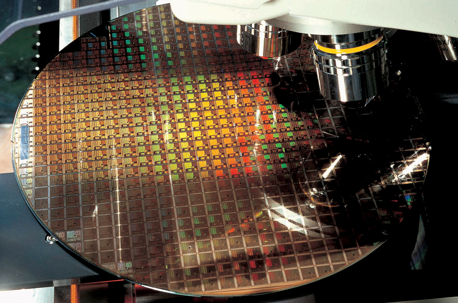
TSMC’s Arizona fab, christened Fab21, will occupy at least 1,100 acres of land in Phoenix, Arizona, and will churn out tens of thousands of semiconductor wafers in the 5 nm class for the Taiwanese company’s customers around the world (initial output is expected at 20K wafers, just short of the 25K TSMC considers for its GigaFab nomenclature). This includes chips fabricated in the N5, N5P, and even N4 processes.
N5 and N5P have been tapped by both AMD and Apple, powering AMD’s already-announced Zen 4 CPUs and chiplet-based RDNA3 GPUs (which are sure to make it into our Best Picks for graphics cards), as well as Apple’s evolution of its original Apple Silicon, the M2 SoC (System-on-Chip).
TSMC Phoenix fab construction site on March 2nd vs TSMC Phoenix fab construction site today pic.twitter.com/5a8Vn8et7yDecember 29, 2021
Naturally, Qualcomm and Nvidia are also prospective clients for TSMC’s chips; the former is all but a given, especially considering how it recently moved production of its Snapdragon chips from Samsung to TSMC. It’s hard to imagine the company going with another foundry for its upcoming Nuvia Arm-based chips as well, with which the company wants to officially go toe-to-toe against the Intels and AMDs of the world. Nvidia still hasn’t confirmed that its next-gen consumer GPUs will use TSMC’s manufacturing, but its monstrous, data center-focussed Hopper does.
The Arizona fab is of strategic importance for TSMC’s bid to increase its 5 nm output beyond the 25% already planned for 2022. Intel has also become a customer of the Taiwanese manufacturer — Intel CEO Pat Gelsinger recently visited Taiwan in a bid to secure additional capacity for the company’s silicon designs.
It’s also a bid for the company to insulate its IP and production capacities from geopolitical concerns, considering the proximity of China — where some believe the country should seize TSMC for its treasure trove of technological innovation.
TSMC’s construction on its latest semiconductor fabrication facility in Arizona is progressing at breakneck speeds. Thanks to the photographic reporting skills of Matt Schrader on Twitter, we can now witness the incredible construction rate for what will soon become one of the most advanced silicon fabrication facilities across the world.
The construction grounds literally went from tumbleweeds to factory shells in under six months, spelling a good pace for the factory’s expected spin-up in early 2024. That’s what a cool $10 to $12 billion can do, as you can see when you expand the below tweet.
TSMC’s Arizona fab, christened Fab21, will occupy at least 1,100 acres of land in Phoenix, Arizona, and will churn out tens of thousands of semiconductor wafers in the 5 nm class for the Taiwanese company’s customers around the world (initial output is expected at 20K wafers, just short of the 25K TSMC considers for its GigaFab nomenclature). This includes chips fabricated in the N5, N5P, and even N4 processes.
N5 and N5P have been tapped by both AMD and Apple, powering AMD’s already-announced Zen 4 CPUs and chiplet-based RDNA3 GPUs (which are sure to make it into our Best Picks for graphics cards), as well as Apple’s evolution of its original Apple Silicon, the M2 SoC (System-on-Chip).
TSMC Phoenix fab construction site on March 2nd vs TSMC Phoenix fab construction site today pic.twitter.com/5a8Vn8et7yDecember 29, 2021
Naturally, Qualcomm and Nvidia are also prospective clients for TSMC’s chips; the former is all but a given, especially considering how it recently moved production of its Snapdragon chips from Samsung to TSMC. It’s hard to imagine the company going with another foundry for its upcoming Nuvia Arm-based chips as well, with which the company wants to officially go toe-to-toe against the Intels and AMDs of the world. Nvidia still hasn’t confirmed that its next-gen consumer GPUs will use TSMC’s manufacturing, but its monstrous, data center-focussed Hopper does.
The Arizona fab is of strategic importance for TSMC’s bid to increase its 5 nm output beyond the 25% already planned for 2022. Intel has also become a customer of the Taiwanese manufacturer — Intel CEO Pat Gelsinger recently visited Taiwan in a bid to secure additional capacity for the company’s silicon designs.
It’s also a bid for the company to insulate its IP and production capacities from geopolitical concerns, considering the proximity of China — where some believe the country should seize TSMC for its treasure trove of technological innovation.
Denial of responsibility! Techno Blender is an automatic aggregator of the all world’s media. In each content, the hyperlink to the primary source is specified. All trademarks belong to their rightful owners, all materials to their authors. If you are the owner of the content and do not want us to publish your materials, please contact us by email – [email protected]. The content will be deleted within 24 hours.