
‘India will soon make equipment for semiconductor manufacturing’, ET Auto
India will soon start making equipment for semiconductor manufacturing, Union telecom and IT minister Ashwini Vaishnaw said on Saturday.
“The entire semiconductor ecosystem of fabs, ATMP units, chemicals, gases, substrate, consumables and equipment for semiconductor manufacturing will be made in India,” he said.
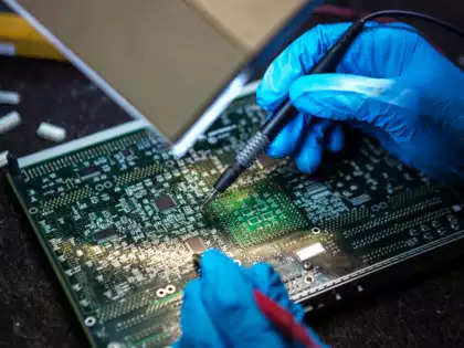
He was speaking at the inauguration of American chip equipment supplier Applied Materials’ India Validation Centre in Bengaluru which was set up at a cost of USD 20 million.
Such labs are present in the US, Singapore, China and Korea. The India Validation Centre will have a workforce of 500 people.
The company last year announced that it will set up an engineering centre in Bengaluru with a total investment of USD 400 million over four years to develop and commercialise technologies for semiconductor manufacturing equipment.
Vaishnaw said that the components that were earlier imported from Japan, Korea and Taiwan are being made by the company here now.
“Today, all the four agreements made during the Prime Minister’s state visit to the US have been materialised,” Vaishnaw said.
The construction of Micron’s ATMP has commenced. In addition, LAM Research’s proposal to deliver a virtual nano fabrication environment through its Semiverse Solutions to train semiconductor engineers in India has also started.
“The first training course in the Indian Institute of Science has started with 35 students,” the minister said. The third agreement was in relation to a centre of Applied Materials to be set up in India, he said. “This has also fructified with a centre of the company being set up here,” he said.
A design centre of Advanced Micro Devices (AMD) was also to be set up in India. “A few months back, I inaugurated the design centre of AMD in Bengaluru,” Vaishnaw said.
A first for 300 mm wafer processing
Sonny Kunnakkat, managing director, Advanced Manufacturing Technology, Worldwide Operations, Applied Materials, told ET that this is the first private facility in India that will process 300 mm wafers.
So far, 200 mm wafers have been processed in India.
“We used to have a 300 mm processing facility in the Indian Institute of Technology but that was academic. This is a commercial one. We will do our own development work. The wafers that we make are not sold as we are an equipment company and not a chip company. Our equipment here will go to our customers to make their chips,” Kunnakkat said.
The change rate of the equipment is very fast, he said. Equipment and components must be continuously developed with evolving customer challenges. “That is the kind of development that will be done here,” he said.

India will soon start making equipment for semiconductor manufacturing, Union telecom and IT minister Ashwini Vaishnaw said on Saturday.
“The entire semiconductor ecosystem of fabs, ATMP units, chemicals, gases, substrate, consumables and equipment for semiconductor manufacturing will be made in India,” he said.
He was speaking at the inauguration of American chip equipment supplier Applied Materials’ India Validation Centre in Bengaluru which was set up at a cost of USD 20 million.
Such labs are present in the US, Singapore, China and Korea. The India Validation Centre will have a workforce of 500 people.
The company last year announced that it will set up an engineering centre in Bengaluru with a total investment of USD 400 million over four years to develop and commercialise technologies for semiconductor manufacturing equipment.
Vaishnaw said that the components that were earlier imported from Japan, Korea and Taiwan are being made by the company here now.
“Today, all the four agreements made during the Prime Minister’s state visit to the US have been materialised,” Vaishnaw said.
The construction of Micron’s ATMP has commenced. In addition, LAM Research’s proposal to deliver a virtual nano fabrication environment through its Semiverse Solutions to train semiconductor engineers in India has also started.
“The first training course in the Indian Institute of Science has started with 35 students,” the minister said. The third agreement was in relation to a centre of Applied Materials to be set up in India, he said. “This has also fructified with a centre of the company being set up here,” he said.
A design centre of Advanced Micro Devices (AMD) was also to be set up in India. “A few months back, I inaugurated the design centre of AMD in Bengaluru,” Vaishnaw said.
A first for 300 mm wafer processing
Sonny Kunnakkat, managing director, Advanced Manufacturing Technology, Worldwide Operations, Applied Materials, told ET that this is the first private facility in India that will process 300 mm wafers.
So far, 200 mm wafers have been processed in India.
“We used to have a 300 mm processing facility in the Indian Institute of Technology but that was academic. This is a commercial one. We will do our own development work. The wafers that we make are not sold as we are an equipment company and not a chip company. Our equipment here will go to our customers to make their chips,” Kunnakkat said.
The change rate of the equipment is very fast, he said. Equipment and components must be continuously developed with evolving customer challenges. “That is the kind of development that will be done here,” he said.
Denial of responsibility! Techno Blender is an automatic aggregator of the all world’s media. In each content, the hyperlink to the primary source is specified. All trademarks belong to their rightful owners, all materials to their authors. If you are the owner of the content and do not want us to publish your materials, please contact us by email – [email protected]. The content will be deleted within 24 hours.