
The Future of AI Chips
The interest and investment in AI is skyrocketing, and generative AI is fueling it. Over one-third of CxOs have reportedly already embraced GenAI in their operations, with nearly half preparing to invest in it.
What’s powering it all, AI chips used to receive less attention. Up to the moment, OpenAI’s Sam Altman claimed he wants to raise up to $7 trillion for a “wildly ambitious” tech project to boost the world’s chip capacity. Geopolitics and sensationalism aside, however, keeping an eye on AI chips means being aware of today’s blockers and tomorrow’s opportunities.
According to a recent study by IMARC, the global AI chip market is expected to reach $89.6 Billion by 2029. The demand for AI chips has increased substantially over time. Growth in AI technology, rising demand for AI chips in consumer electronics, and AI chip innovation all contribute to this forecast.
Few people have more insights to share on AI hardware than Tony Pialis, CEO and co-founder of Alphawave. In an extensive conversation, Pialis shared his insider’s perspective on the AI chip landscape, the transformative rise of chiplets, specialized hardware for training and inference, emerging directions like analog and optical computing, and much more.
An AI Leader Behind the Scenes
Pialis is a semiconductor serial entrepreneur. He has previously founded and successfully sold two startups: Snowbush Microelectronics and V Semiconductor Inc. V Semiconductor was acquired by Intel in 2012, where Pialis spent a few years as the Vice President of Analog and Mixed-Signal IP.
Pialis co-founded AlphaWave in 2017 with the goal of becoming “the next great semiconductor company.” Alphawave went public in 2021 with an impressive market cap of $4.5 billion. The company’s core products include silicon IP, chips, custom silicon, and high-speed interconnect technology tailored for major hyperscaler customers like Google, Microsoft, Amazon, and Meta.
Alphawave is an AI leader behind the scenes, powering hyperscalers, and founded on a couple of key, premises that Pialis laid out.
First, the major players in terms of scaling out data centers and computing these days are no longer the Ciscos of the world. It’s transitioned to Hyperscalers – the Googles, Microsofts, Amazons, and Metas. Hyperscalers have internal design capability, and they also build their own servers, networks, data centers, and campuses.
Second, the major challenge facing AI moving forward is not computing. Pialis’ view is that the ability to design and implement computing is there. The challenge is the connectivity needed to connect the compute in order to process all of the data. This is what AlphaWave is focusing on.
The Explosion of Specialized AI Hardware
While consumer apps like ChatGPT drove the initial hype cycle in 2023, enterprise adoption reports are mixed. However, according to Pialis, the AI semiconductor sector has seen an enormous explosion of investment and new design starts in the second half of 2023 across industries and geographies.
Pialis cited major national initiatives around building domestic AI chip capabilities in the US, Canada, UK, France, Germany, Korea, Taiwan and Japan. After years of relying largely on NVIDIA, governments want to foster their own chip industries to reduce strategic dependence on any one vendor. While NVIDIA CEO Jensen Huang also says that every country needs Sovereign AI, it does not seem like this also includes the hardware layer.
Pialis believes this surging demand is spurring not just startups but also tech giants to develop specialized training and inference hardware. In his view, not every organization could or should develop its own AI model, but that’s bound to change.
“Over time, AI will inevitably progress to be something like a utility, where hyperscalers will provide access to all of the compute power, like electricity. I think it will be reasonably priced. Anyone will be able to use this utility to train, develop, optimize, and deploy their own models.
But there’s going to be a lot of profit taking between now and then, and who knows how long it’ll take to eventually reach that state”, said Pialis.
Leaders, Dark Horses, and Rising Starts in the AI Chip Race
Few people would disagree that NVIDIA is clearly the dominant force in AI accelerators today, and Pialis shares this view. He sees AMD as a strong second place, and praised CEO Lisa Su for her leadership. Others, such as Ben Lorica, also see favorable winds for AMD in the GenAI chip market.
But Pialis cautioned not to underestimate Intel, calling it a dark horse which could still prove highly formidable in this market. More specifically, Pialis spoke highly of Intel’s Habana acqui-hired division led by David Dahan.
Having worked at Intel, Pialis has an insider view. Having covered Habana, met Dahan, and kept track of their MLPerf results, we tend to agree. Dahan helped architect new Intel processors that have showcased performance exceeding NVIDIA’s latest GPUs on key benchmarks.
However, performance is not everything. As Pialis also noted, NVIDIA’s software platform, including CUDA, gives it a huge advantage in the AI chip segment. The ecosystem effects are strong as engineers and researchers develop optimized frameworks and models for NVIDIA’s architecture.
But there is potential for alternatives; for example, building upon AMD’s hardware and software stack. Pialis opined that a rule of thumb for AI hardware companies is that for every hardware engineer, they need 2-3 software engineers. So, even though there’s a lot of talk about NVIDIA and hardware, the vast majority of the investment actuallyDark HorsesRising Stars goes into the software.
This was confirmed by NVIDIA’s Dave Salvator. At the last MLPerf results briefing for 2023, Salvator said that NVIDIA has twice as many software engineers as hardware engineers. That’s not at all by accident, as he emphasized.
Pialis sees far more potential for challengers in the inference accelerator market. The reason is that standards are still emerging in that area. As OctoML’s Luis Ceze shared, there’s vLLM for LLM serving, MLC-LLM for portable deployment, LoRAX, and Punica for multiplexed fined-tuned model inference. Inference is, in fact, a bigger market than training, as Pialis noted.
“There’s so much focus on training, large models, and the cost of training. But it’s a deployment where we all benefit from, on the inference side. That needs a significant scale. That needs a different solution. More chips will inevitably be sold on the inference side than the training side. I’m sure business plans also improve with that increase in volume”, Pialis said.
Startups like Groq and Tenstorrent are attracting significant funding, and so are companies from countries like the UK, Korea, and China trying to reduce reliance on US firms. As far as hyperscalers go, Pialis sees Amazon and Google as being neck to neck, with Microsoft showing strong momentum, and Meta being behind and rumored to acquire one of the smaller startups.
The Chiplet Technological Revolution
One of the biggest transformations underway in semiconductors, according to Pialis, is the shift to chiplets. Previously, progress meant integrating more and more functionality into a single monolithic chip. But transistor dimensions are now down to ~5 atoms wide, and even tiny defects can ruin a whole chip.
Pialis shared an anecdote from his own experience to highlight this. As he related, when he visited OpenAI at some point, he saw a bunch of engineers on their knees praying in front of servers. Not because they were “feeling the AGI” but rather because they didn’t want the model they were training to crash.
Some of us may have first heard about chiplets in the context of the China-US trade war that spills over to technology. Chiplets are a key element in the strategy of both China and the US.
For Pialis, “Chiplets are another technological revolution to deal with the problem that God has thrown at us.”
The challenges of physics at the nanoscale mean we may be reaching the limits of current hardware technology.
This may sound like a wild appeal to the supernatural, but it has more to do with the challenges of physics at nanoscale.
“When we build transistors, which are the basic building blocks of any integrated circuit, we’re stacking atoms. When you’re stacking atoms, the laws of probability, the laws of averaging, fall apart because now it’s two atoms rather than hundreds of atoms and electrons. So what you get is defects”, Pialis explained.
Chiplets are an innovative solution to this nanoscale physics challenge. Rather than one giant chip, designs are split into smaller Lego-like chiplets that can be connected through advanced packaging. This modularity lets chipmakers avoid throwing out entire devices due to one small flaw. The benefits, Pialis said, are important for both makers and buyers.
“Silicon is no longer the foundation of leading edge semiconductors; it’s the package. Silicon is now something that is a component on this packaging. There’s been a lot of talk about semiconductor supply chains. There’s a lot of silicon capacity now. Where there’s still very little to no capacity is on the packaging, specifically for designs built using chiplets”, Pialis noted.
Chiplets as Lego Building Blocks
However, there is a standout example of an AI hardware company that seems to be successful despite going the opposite way: Cerebras. Cerebras is known for its wafer-scale hardware. Pialis was positive that Cerebras is going to encounter the same defects as everyone else. The difference with Cerebras is they have redundancy.
A wafer is like a panel, Pialis noted. Cerebras doesn’t even cut the panel. What they do is they have software that works around the defects. Fundamentally, they’re using silicon as the foundation rather than packaging. They have multiple chips that are arrayed, but they’re not cut. They just connect on the wafer. It definitely is a different approach.
However, Pialis added, there are advantages to cutting things up. Imagine a vendor like Intel is trying to build different units, such as a CPU, a GPU, a DPU, or a networking device. By breaking things up into smaller pieces, they become like Lego building blocks.
So you can have a processor core chiplet, a PCI Express connectivity chiplet, an Ethernet networking chiplet, a DDR memory I/O chiplet, a memory I/O chiplet. These chiplets can be mixed and matched in a package to build out an entire product portfolio. Pialis thinks that from a design complexity and upfront investment perspective, that’s a winning formula.
Pialis sees massive benefits in chiplets, reducing costs by over 60% and power consumption by 40%. This is a major incentive for hyperscale data centers. While he sees Apple, AMD and Intel leading in chiplets today, Pialis believes chiplets will soon become essential for any company focused on leading edge hardware.
Software and Chiplet Modularity, Composability, and Programmability
Drawing parallels from the world of software engineering, one can wonder how come the modularity that chiplets bring to the table did not prevail earlier. But in hardware, up to now the winners were the ones that could integrate into a monolithic device the most.
The reason is that this drove down cost, which Pialis noted has created “a maniacal focus on integration.” However, as we now approach the dimensions of a single atom, the manufacturing cost eclipses the cost of integration. But even in software, excessive modularity can also incur excessive overhead.
Pialis expects that some hardware vendors may take the chiplet approach too far. If functionality is broken into too many tiny pieces, the cost of integrating all of these becomes limiting. So, ultimately, it’ll be a hybrid approach that wins. There are two ways of splitting things up with chiplets. 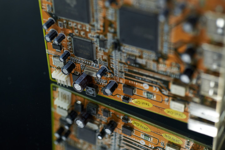
Up to now, the winners in hardware were the ones that could integrate into a monolithic device the most. But that’s changing.
The first way of building chiplets is building a single Lego block, mirroring it over and over with the same functionality, and they just talk to each other. That seems more akin to the “traditional” approach. However, one may wonder how these identical chiplet building blocks can be synthesized. The answer is, again, software.
Different packages can be composed for different needs, based on the same chiplet, using software. For example, multiples of 1, 2, 4, or 8 chiplets. The same silicon, just packaged differently, priced differently, and with different software to leverage the incremental compute and memory bandwidth associated with these devices.
The other way of building chiplets is by splitting and cutting, creating Lego blocks for different types of functionality. This creates chiplets like a compute Lego block, a training I/O Lego block, a network I/O Lego block, and so on. Pialis sees more momentum behind this approach, as reusable Lego blocks can accelerate other products, too.
Analog AI, Optical Computing, and AI-Assisted Hardware Design
Chiplets may be the immediate way forward. But at a time when power-hungry digital accelerators like GPUs dominate, Pialis claims there are other ways. And they involve a radical break with the current paradigm.
AI needs massively parallelized arithmetic processing, and binary is the dominant approach for this. Using binary computing, numbers are represented as ones and zeros, and floating point arithmetic is done by defining precision and range.
In analog arithmetic processing, floating point can be represented via voltages or currents. In theory, that may have infinite precision. In the real world where noise exists, that may yield less precision. But that may well work for Edge AI applications. Using very small currents keeps things operating at low power.
There’s another form of compute that some companies are investing in: optical compute for arithmetic. Optical compute uses the properties of optics to implement what are called MACs (multiply and accumulate functionality) which is the core of any arithmetic unit. This results in even lower power demands.
Pialis noted that analog and optical approaches are attracting billions in investment to meet specialized needs around computational scale, energy efficiency, and precision. However, it remains unclear if analog techniques can scale effectively to match digital compute for cutting edge AI models. There is active debate on this question in the hardware community.
Finally, there’s also the question of using AI to help design hardware to power AI. Pialis said that the most effective hardware designers these days are the best software developers. But if AI models can be trained by leveraging the wealth of their experience, that may bring about a sea change.
While the road ahead is complex, Pialis believes the fundamental principles of engineering are timeless. Hopefully, that translates to something that does not end up draining the world’s energy and resources on the promise of future gains to be made.
The interest and investment in AI is skyrocketing, and generative AI is fueling it. Over one-third of CxOs have reportedly already embraced GenAI in their operations, with nearly half preparing to invest in it.
What’s powering it all, AI chips used to receive less attention. Up to the moment, OpenAI’s Sam Altman claimed he wants to raise up to $7 trillion for a “wildly ambitious” tech project to boost the world’s chip capacity. Geopolitics and sensationalism aside, however, keeping an eye on AI chips means being aware of today’s blockers and tomorrow’s opportunities.
According to a recent study by IMARC, the global AI chip market is expected to reach $89.6 Billion by 2029. The demand for AI chips has increased substantially over time. Growth in AI technology, rising demand for AI chips in consumer electronics, and AI chip innovation all contribute to this forecast.
Few people have more insights to share on AI hardware than Tony Pialis, CEO and co-founder of Alphawave. In an extensive conversation, Pialis shared his insider’s perspective on the AI chip landscape, the transformative rise of chiplets, specialized hardware for training and inference, emerging directions like analog and optical computing, and much more.
An AI Leader Behind the Scenes
Pialis is a semiconductor serial entrepreneur. He has previously founded and successfully sold two startups: Snowbush Microelectronics and V Semiconductor Inc. V Semiconductor was acquired by Intel in 2012, where Pialis spent a few years as the Vice President of Analog and Mixed-Signal IP.
Pialis co-founded AlphaWave in 2017 with the goal of becoming “the next great semiconductor company.” Alphawave went public in 2021 with an impressive market cap of $4.5 billion. The company’s core products include silicon IP, chips, custom silicon, and high-speed interconnect technology tailored for major hyperscaler customers like Google, Microsoft, Amazon, and Meta.
Alphawave is an AI leader behind the scenes, powering hyperscalers, and founded on a couple of key, premises that Pialis laid out.
First, the major players in terms of scaling out data centers and computing these days are no longer the Ciscos of the world. It’s transitioned to Hyperscalers – the Googles, Microsofts, Amazons, and Metas. Hyperscalers have internal design capability, and they also build their own servers, networks, data centers, and campuses.
Second, the major challenge facing AI moving forward is not computing. Pialis’ view is that the ability to design and implement computing is there. The challenge is the connectivity needed to connect the compute in order to process all of the data. This is what AlphaWave is focusing on.
The Explosion of Specialized AI Hardware
While consumer apps like ChatGPT drove the initial hype cycle in 2023, enterprise adoption reports are mixed. However, according to Pialis, the AI semiconductor sector has seen an enormous explosion of investment and new design starts in the second half of 2023 across industries and geographies.
Pialis cited major national initiatives around building domestic AI chip capabilities in the US, Canada, UK, France, Germany, Korea, Taiwan and Japan. After years of relying largely on NVIDIA, governments want to foster their own chip industries to reduce strategic dependence on any one vendor. While NVIDIA CEO Jensen Huang also says that every country needs Sovereign AI, it does not seem like this also includes the hardware layer.
Pialis believes this surging demand is spurring not just startups but also tech giants to develop specialized training and inference hardware. In his view, not every organization could or should develop its own AI model, but that’s bound to change.
“Over time, AI will inevitably progress to be something like a utility, where hyperscalers will provide access to all of the compute power, like electricity. I think it will be reasonably priced. Anyone will be able to use this utility to train, develop, optimize, and deploy their own models.
But there’s going to be a lot of profit taking between now and then, and who knows how long it’ll take to eventually reach that state”, said Pialis.
Leaders, Dark Horses, and Rising Starts in the AI Chip Race
Few people would disagree that NVIDIA is clearly the dominant force in AI accelerators today, and Pialis shares this view. He sees AMD as a strong second place, and praised CEO Lisa Su for her leadership. Others, such as Ben Lorica, also see favorable winds for AMD in the GenAI chip market.
But Pialis cautioned not to underestimate Intel, calling it a dark horse which could still prove highly formidable in this market. More specifically, Pialis spoke highly of Intel’s Habana acqui-hired division led by David Dahan.
Having worked at Intel, Pialis has an insider view. Having covered Habana, met Dahan, and kept track of their MLPerf results, we tend to agree. Dahan helped architect new Intel processors that have showcased performance exceeding NVIDIA’s latest GPUs on key benchmarks.
However, performance is not everything. As Pialis also noted, NVIDIA’s software platform, including CUDA, gives it a huge advantage in the AI chip segment. The ecosystem effects are strong as engineers and researchers develop optimized frameworks and models for NVIDIA’s architecture.
But there is potential for alternatives; for example, building upon AMD’s hardware and software stack. Pialis opined that a rule of thumb for AI hardware companies is that for every hardware engineer, they need 2-3 software engineers. So, even though there’s a lot of talk about NVIDIA and hardware, the vast majority of the investment actuallyDark HorsesRising Stars goes into the software.
This was confirmed by NVIDIA’s Dave Salvator. At the last MLPerf results briefing for 2023, Salvator said that NVIDIA has twice as many software engineers as hardware engineers. That’s not at all by accident, as he emphasized.
Pialis sees far more potential for challengers in the inference accelerator market. The reason is that standards are still emerging in that area. As OctoML’s Luis Ceze shared, there’s vLLM for LLM serving, MLC-LLM for portable deployment, LoRAX, and Punica for multiplexed fined-tuned model inference. Inference is, in fact, a bigger market than training, as Pialis noted.
“There’s so much focus on training, large models, and the cost of training. But it’s a deployment where we all benefit from, on the inference side. That needs a significant scale. That needs a different solution. More chips will inevitably be sold on the inference side than the training side. I’m sure business plans also improve with that increase in volume”, Pialis said.
Startups like Groq and Tenstorrent are attracting significant funding, and so are companies from countries like the UK, Korea, and China trying to reduce reliance on US firms. As far as hyperscalers go, Pialis sees Amazon and Google as being neck to neck, with Microsoft showing strong momentum, and Meta being behind and rumored to acquire one of the smaller startups.
The Chiplet Technological Revolution
One of the biggest transformations underway in semiconductors, according to Pialis, is the shift to chiplets. Previously, progress meant integrating more and more functionality into a single monolithic chip. But transistor dimensions are now down to ~5 atoms wide, and even tiny defects can ruin a whole chip.
Pialis shared an anecdote from his own experience to highlight this. As he related, when he visited OpenAI at some point, he saw a bunch of engineers on their knees praying in front of servers. Not because they were “feeling the AGI” but rather because they didn’t want the model they were training to crash.
Some of us may have first heard about chiplets in the context of the China-US trade war that spills over to technology. Chiplets are a key element in the strategy of both China and the US.
For Pialis, “Chiplets are another technological revolution to deal with the problem that God has thrown at us.”
The challenges of physics at the nanoscale mean we may be reaching the limits of current hardware technology.
This may sound like a wild appeal to the supernatural, but it has more to do with the challenges of physics at nanoscale.
“When we build transistors, which are the basic building blocks of any integrated circuit, we’re stacking atoms. When you’re stacking atoms, the laws of probability, the laws of averaging, fall apart because now it’s two atoms rather than hundreds of atoms and electrons. So what you get is defects”, Pialis explained.
Chiplets are an innovative solution to this nanoscale physics challenge. Rather than one giant chip, designs are split into smaller Lego-like chiplets that can be connected through advanced packaging. This modularity lets chipmakers avoid throwing out entire devices due to one small flaw. The benefits, Pialis said, are important for both makers and buyers.
“Silicon is no longer the foundation of leading edge semiconductors; it’s the package. Silicon is now something that is a component on this packaging. There’s been a lot of talk about semiconductor supply chains. There’s a lot of silicon capacity now. Where there’s still very little to no capacity is on the packaging, specifically for designs built using chiplets”, Pialis noted.
Chiplets as Lego Building Blocks
However, there is a standout example of an AI hardware company that seems to be successful despite going the opposite way: Cerebras. Cerebras is known for its wafer-scale hardware. Pialis was positive that Cerebras is going to encounter the same defects as everyone else. The difference with Cerebras is they have redundancy.
A wafer is like a panel, Pialis noted. Cerebras doesn’t even cut the panel. What they do is they have software that works around the defects. Fundamentally, they’re using silicon as the foundation rather than packaging. They have multiple chips that are arrayed, but they’re not cut. They just connect on the wafer. It definitely is a different approach.
However, Pialis added, there are advantages to cutting things up. Imagine a vendor like Intel is trying to build different units, such as a CPU, a GPU, a DPU, or a networking device. By breaking things up into smaller pieces, they become like Lego building blocks.
So you can have a processor core chiplet, a PCI Express connectivity chiplet, an Ethernet networking chiplet, a DDR memory I/O chiplet, a memory I/O chiplet. These chiplets can be mixed and matched in a package to build out an entire product portfolio. Pialis thinks that from a design complexity and upfront investment perspective, that’s a winning formula.
Pialis sees massive benefits in chiplets, reducing costs by over 60% and power consumption by 40%. This is a major incentive for hyperscale data centers. While he sees Apple, AMD and Intel leading in chiplets today, Pialis believes chiplets will soon become essential for any company focused on leading edge hardware.
Software and Chiplet Modularity, Composability, and Programmability
Drawing parallels from the world of software engineering, one can wonder how come the modularity that chiplets bring to the table did not prevail earlier. But in hardware, up to now the winners were the ones that could integrate into a monolithic device the most.
The reason is that this drove down cost, which Pialis noted has created “a maniacal focus on integration.” However, as we now approach the dimensions of a single atom, the manufacturing cost eclipses the cost of integration. But even in software, excessive modularity can also incur excessive overhead.
Pialis expects that some hardware vendors may take the chiplet approach too far. If functionality is broken into too many tiny pieces, the cost of integrating all of these becomes limiting. So, ultimately, it’ll be a hybrid approach that wins. There are two ways of splitting things up with chiplets.
Up to now, the winners in hardware were the ones that could integrate into a monolithic device the most. But that’s changing.
The first way of building chiplets is building a single Lego block, mirroring it over and over with the same functionality, and they just talk to each other. That seems more akin to the “traditional” approach. However, one may wonder how these identical chiplet building blocks can be synthesized. The answer is, again, software.
Different packages can be composed for different needs, based on the same chiplet, using software. For example, multiples of 1, 2, 4, or 8 chiplets. The same silicon, just packaged differently, priced differently, and with different software to leverage the incremental compute and memory bandwidth associated with these devices.
The other way of building chiplets is by splitting and cutting, creating Lego blocks for different types of functionality. This creates chiplets like a compute Lego block, a training I/O Lego block, a network I/O Lego block, and so on. Pialis sees more momentum behind this approach, as reusable Lego blocks can accelerate other products, too.
Analog AI, Optical Computing, and AI-Assisted Hardware Design
Chiplets may be the immediate way forward. But at a time when power-hungry digital accelerators like GPUs dominate, Pialis claims there are other ways. And they involve a radical break with the current paradigm.
AI needs massively parallelized arithmetic processing, and binary is the dominant approach for this. Using binary computing, numbers are represented as ones and zeros, and floating point arithmetic is done by defining precision and range.
In analog arithmetic processing, floating point can be represented via voltages or currents. In theory, that may have infinite precision. In the real world where noise exists, that may yield less precision. But that may well work for Edge AI applications. Using very small currents keeps things operating at low power.
There’s another form of compute that some companies are investing in: optical compute for arithmetic. Optical compute uses the properties of optics to implement what are called MACs (multiply and accumulate functionality) which is the core of any arithmetic unit. This results in even lower power demands.
Pialis noted that analog and optical approaches are attracting billions in investment to meet specialized needs around computational scale, energy efficiency, and precision. However, it remains unclear if analog techniques can scale effectively to match digital compute for cutting edge AI models. There is active debate on this question in the hardware community.
Finally, there’s also the question of using AI to help design hardware to power AI. Pialis said that the most effective hardware designers these days are the best software developers. But if AI models can be trained by leveraging the wealth of their experience, that may bring about a sea change.
While the road ahead is complex, Pialis believes the fundamental principles of engineering are timeless. Hopefully, that translates to something that does not end up draining the world’s energy and resources on the promise of future gains to be made.
Denial of responsibility! Techno Blender is an automatic aggregator of the all world’s media. In each content, the hyperlink to the primary source is specified. All trademarks belong to their rightful owners, all materials to their authors. If you are the owner of the content and do not want us to publish your materials, please contact us by email – [email protected]. The content will be deleted within 24 hours.